Intel FPGA - Leading FPGA, SoC and Power
- September 10, 2021
 Interface - CODECs
 AC DC Converters, Offline Switchers
 DC Switching Regulators
 DC DC Switching Controllers
 Specialized Interfaces
 Laser Drivers
 Linear - Video Processing
 Linear Voltage Regulators
 Microcontrollers
 Memory ICs
 Instrumentation Amplifier
 Motor Drivers and Controllers
 Power Supply Controllers, Monitors
 Specialized Power Management IC
 Clock Generators and Frequency Synthesizers
 Encoders, Decoders, Converters
 FPGAs (Field Programmable Gate Array)
 Linear Comparators
 Voltage Reference
 Special Purpose Voltage Regulators
 Battery Management
 Full, Half-Bridge Drivers
 Power Distribution Switches, Load Drivers
 Supervisors
 Current Regulation/Management
 Audio Amplifiers
 Display Drivers
 LED Drivers
 Gate Drivers
 Analog Multipliers, Dividers
 RMS to DC Converters
 Gates and Inverters
 Video Amps and Modules
 Buffers, Drivers, Receivers, Transceivers
 Digital to Analog Converters (DAC)
 Digital Potentiometers
 Analog to Digital Converters (ADC)
 Signal Switches, Multiplexers, Decoders
 Interface - Drivers, Receivers, Transceivers
 Analog Switches, Multiplexers, Demultiplexers
 Voltage Translators, Level Shifters
 Programmable Timers and Oscillators
 Multivibrators
 Gates and Inverters - Multi-Function, Configurable
 Hot Swap Controllers
 Ideal Diode & ORing Controllers
 Flip-Flop
 Specialty Logic ICs
 Signal Buffers, Repeaters, Splitters
 Special Purpose Linear Amplifiers
 Specialized ICs
 Lighting, Ballast Controllers
 Linear Regulator Controllers
 Clock Buffers, Drivers
 Special Purpose Audio ICs
 Real Time Clocks
 Filters - Active
 Thermal Management
 I/O Expanders
 Clock/Timing - Delay Lines
 Sensor and Detector Interfaces
 Power Over Ethernet (PoE) Controllers
 Application-Specific Clock/Timing ICs
 Memory - Configuration Proms for FPGAs
 Counters, Dividers
 Network Interface Card (NIC)
 PFC (Power Factor Correction)
 Memory Controllers
 V/F and F/V Converters
 Voltage Regulators - Linear + Switching
 ADCs/DACs
 Telecom Interface ICs
 DSP (Digital Signal Processors)
 Application Specific Microcontrollers
 CPLDs (Complex Programmable Logic Devices)
 Microprocessors
 Direct Digital Synthesis (DDS)
 Signal Terminators
 Universal Asynchronous Receiver Transmitter
 Serializer/Deserializer (SerDes)
 Touch Screen Controllers
 Universal Bus Functions
 Energy Metering
 FIFOs Memory
 Analog Front End (AFE)
 Latches
 Shift Registers
 Voice Record and Playback
 Modems - ICs and Modules
 Parity Generators and Checkers
 PLDs (Programmable Logic Device)
 Logic Comparators
 Clock/Timing - IC Batteries
 FPGA with Microcontrollers
 Microcontroller or Microprocessor Modules
 Memory - Batteries
 Accessories
 System On Chip (SoC)
 Configuration Proms for FPGAs
 Capacitive Touch Sensors, Proximity Sensor ICs
 Single
 Power Driver Modules
 Thyristors Modules
 IGBTs Modules
 I/O Relay Module Racks
 I/O Relay Modules
 Board Mount AC DC Converters
 Off-board DC DC Converters
 Board Mount LED Drivers
 Mosfets
 Power Modules
 Power Semiconductor Accessories
 Thyristors
 Transducers
 Transistors
 Triacs
 AC DC Configurable Power Supply Modules
 DC to AC Inverters
 Memory Modules
 Memory Cards
 Specialized Modules
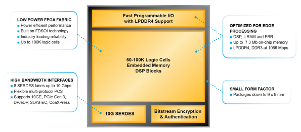
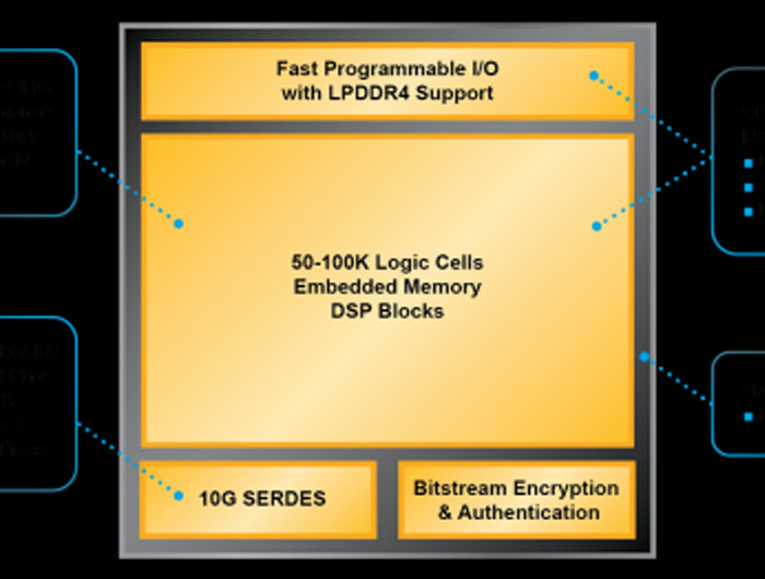
The Certus Pro-NX family sits above the current range with 40,000 logic cells and provides 10Gbit/s Ethernet and Gen 3 PCIe interfaces.
“The Pro-NX starts at 50,000 logic cells so it is targeting the next class up,” says JuJu Joyce, product marketing manager at Lattice Semiconductor. The Pro-NX will start shipping in volume in the second half of next year, after the company has launched its next generation of FPGA technology, the Nexus5, in the first half of next year.
The Nexus5 FPGA will be built on the same 28nm FD-SOI CMOS process technology as the current generation, which will limit the ability to boost the cell count.
“We always aim to be price competitive but we are providing more value,” said Joyce. “We see the need for low power for simpler thermal management in harsh environments where many of the edge networks are deployed, in cell towers or environments without airflow with motor control or in a small form factor for Industrial camera module. By building it specifically for this class you get better power efficiency,” he said.
“The higher bandwidth is needed as more data is generated at the edge from the various sensors and these are getting more capable and higher resolution,” he said.
The I/O provides hardened IP for a low power LPDDR4 memory interface and 10.3Gbit/s for 8 lane SERDES and Gen3 PCIe or 10G ethernet connections. It also includes SLVS-EC for sensors, Coaxpress and DisplayPort.
The family of devices also includes up to 7.3Mbit on-chip memory to support machine learning frameworks without having to go off the chip.
“One of the bottlenecks for AI inferencing is on-chip memory to store the weights for the neural nets so to overcome that we have provided 65 percent more on-chip memory so for many of the processing functions you don’t have to rely on external memory that adds additional latency and power,” said Joyce. “We have EBR embedded block RAM of 18Kbits in columns in the fabric and we have large RAM blocks of 512Kbits and those are at the peripheral connected via the standard fabric.” -
The smallest part with the lowest density interface fits into a 9 x 9 mm BGA package with a 0.5mm ball pitch for the tight integration with a temperature rating of -40 to +125C for industrial applications.
The various AI and machine visions stacks will be ported to the new devices and there is an updated version of its Radiant design tool.
The SERDES analysis tools in Radiant 3.0 have been enhanced to accommodate the higher SERDES bandwidths supported by CertusPro-NX devices, and there is improved signal traceability throughout the design flow via the graphical user interface (GUI) to help designers trace a signal between the HDL source to the RTL view, and to the technology view and back again.
Radiant also allows the user to choose between the Lattice Synthesis Engine (LSE) and the Synplify Pro synthesis engine. In Radiant 3.0, timing constraints and timing analysis are unified across both synthesis engines. The timing analysis has been separated from other operations so it can run independently which speeds the iterative design process by helping designers evaluate “what-if” scenarios and re-run timing analysis without having to re-run mapping and place-and-route.
“Lattice Radiant 3.0 design software gives developers an easy-to-follow user experience; the tool leads them through the steps of the development flow, including design creation, importing IP, implementation, bitstream generation, downloading the bitstream onto an FPGA, and debugging,” said Roger Do, Senior Product Line Manager, Software at Lattice Semiconductor.
“Developers with little to no experience working with FPGAs can quickly leverage the automated features of Lattice Radiant. For experienced FPGA developers, Lattice Radiant 3.0 allows for more granular control over FPGA settings if specific optimizations are required,” he said.